JOTS v35n1 - Simulation of a Start-up Manufacturing Facility for Nanopore Arrays
Simulation of a Start-up Manufacturing Facility for Nanopore Arrays
Dennis W. Field
Abstract
Simulation is a powerful tool in developing and troubleshooting manufacturing processes, particularly when considering process flows for manufacturing systems that do not yet exist. Simulation can bridge the gap in terms of setting up full-scale manufacturing for nanotechnology products if limited production experience is an issue. An effective use of simulation software is identified when analyzing a typical manufacturing process flow for anodic aluminum oxide (AAO) nanopore arrays. Simulation models, using the ProModel simulation software, were developed based on production flows, projected process times, and equipment. An attempt was made to realistically estimate process times and capacities, however model outputs, in terms of quantitative values, were found less important than the activities involved in setting up the models. The ability of simulation to help link theory and practice in the classroom may be useful in leading students toward higher levels of intellectual behavior as educators strive to build students’ abilities to apply, analyze, evaluate, and create, rather than simply to remember and understand.
Manufacturing Simulation
Simulation is a powerful tool in developing and troubleshooting manufacturing processes, particularly when considering process flows for manufacturing systems that do not yet exist. As noted by Mebrahtu, Walker, and Mileham (2004, p. 245) : “The lack of clear understanding of the dynamics and interaction of components of modern manufacturing systems calls for the use of simulation as an essential support tool.” Simulation can bridge the gap in terms of setting up full-scale manufacturing for nanotechnology products when limited production experience is an issue. Rohrer (1997) also supports the notion that simulation provides one of the best methods of validating system design if the manufacturing system being modeled does not yet exist.
This project involved an analysis of a typical manufacturing process flow for anodic aluminum oxide (AAO) nanopore arrays. Models using the ProModel simulation software were developed based on production flows, projected process times, and equipment. Boundary values for process flows, times, and equipment capacities were derived from discussions with nanotechnology researchers and from reading published reports ( Argonne National Laboratory, 2004 ; Ba & Li, 2000 ; Hu, Gong, Chen, Yuan, Saito, Grimes, & Kichambare, 2001 ; Jessensky, Müller, & Gösele, 1998 ; Knaack, Redden, & Onellion, 2004 ; Liang, Chik, Yin, Xu, 2002 ; Nam, Seo, Park, Bae, Nam, Park, & Ha, 2004 ; Nasirpouri, Ghorbani, Irajizad, Saedi, Nogaret, 2004 ; Zhang, Chen, Li, & Saito, 2005 ). Regarding quantitative values, however, model outputs were found less important than the activities involved in setting up the models, as powerful “what if ” capability in the software allows process times, capacities, and yields to be easily updated.
Background
Nanotechnology refers to applications involving products or materials with one or more features in the one to one-hundred nanometers range. For comparative purposes, most individual atoms are between one-tenth and one-half of a nanometer in diameter.
Initially, the technologies and process flows involved in the production of AAO nanopore arrays are discussed. These arrays offer cost-effective approaches to create nanoscale features over large areas, and they can be applied to the development and production of other nanotechnology devices, including sensors, memory devices, and filtration and flow membranes.
The base simulation model is then defined, and the advanced simulation software is explored including, among other things, the impact of equipment downtimes, alternative process flows based on variable attributes, and IF-THEN-ELSE operation logic, custom graphics, and costs.
The successful scale up of manufacturing for nanoscale structures and devices is not an easy task. In a report published by the Oak Ridge National Laboratory titled “Nanoscale Science, Engineering and Technology Research Directions,” the authors observed that: “This linking from molecular interactions to nanostructures to functional systems is a fundamental challenge of the first order, both scientifically and technologically” ( n.d. p.70).
Research in nanotechnology is well underway; however, commercial manufacturing operations for nanotechnology products are just beginning to emerge. For example, Thomas Swan & Co announced the United Kingdom’s first commercial manufacturing process for high-purity single-wall carbon nanotubes in April 2004 ( AZoNano, 2005 ).
Anodic Aluminum Oxide Nanopore Arrays
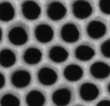
Several products associated with developing technologies were investigated and one, AAO nanopore arrays, was selected around which to develop a manufacturing flow simulation model. AAO nanopore arrays are hexagonally ordered pores fabricated from aluminium using electrochemical processing. The pores can have diameters from 12 nm to 0.1 μm and depths in excess of 60 μm. The pore diameters are controlled by the choice of anodizing voltage and electrolyte. Nanopore arrays can be used to create nanoscale features over large areas, and they can be applied in the development and production of other nanotechnology devices. The potential to use these arrays as a springboard technology to enable cost-effective development of other devices makes them particularly valuable. The process flow for AAO nanopore arrays (see Figure 1) is well documented in a number of previously referenced journal articles and abstracts describing, with some variation, the array fabrication.
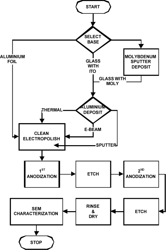
Using the references, a generic example of an AAO array fabrication process involving the following steps was developed. A flowchart of the process is shown in Figure 2. It should be noted that for purposes of the simulation, process times were important, but other process specifications (for example, solution type, temperature, anodizing voltage, and concentrations) did not play a role in the analysis and were not included. More specific process details can be found in the reference list.
- Prepare the substrate. Possible options include aluminium foil, or glass substrates coated with either (a) molybdenum or (b) indium tin oxide and aluminium films. Subsequent process flow is dependent on the type of substrate, and these options are reflected in the software simulation.
- Clean the substrate surface. This could include using a simple solvent or, for some types of substrates, an electropolish.
- Oxidize the aluminium at a constant voltage in an oxalic acid solution at low temperature for approximately 21 hours.
- Remove the initial anodic oxide layer—parts of which are typically distorted—by dipping in an acid mixture at an elevated temperature for 20 hours. This yields a textured pattern of concave depression on the aluminium surface.
- Complete a second anodization of the textured aluminium for approximately 20 minutes. Use the same experimental conditions as the first anodization. This process results in the ordered holes (seen in Figure 1) fabricated from each concave depression.
- Remove the bottom part of the anodic porous alumina membrane by etching it in solution for a short period of time (less than one minute) to form a through-hole membrane.
Simulation Software
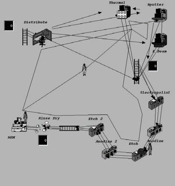
The AAO process flow served as a vehicle to explore various simulation software capabilities. The model included “locations,” which were used to identify and define specific pieces of equipment and buffers, that is “entities” used to define the various products to be processed, and “resources” that covered human resources involved in the process flows. Eleven pieces of equipment and three buffer queues were defined. The equipment included a distribution station to initiate the process flow, three metallization systems (thermal, sputtering, and e-beam), an electropolish station, two anodization and two etch stations, a cleaning station, and a scanning electron microscope. The three entities created to model the three substrates used in this simulation were glass, glass with a thin film of indium tin oxide, and aluminum foil. The three resources included two production operators and one repair and maintenance (R&M) technician. Processing times input to the model ranged from a minimum of one minute for the second etch process to 21 hours for the first anodization. As it turns out, the buffers were not needed during the simulation because the arrival times of the various substrates exceeded the cycle time of the longest process (first anodization); however, it was thought that they might be useful in the future if arrival or processing times or capacities would change. Multiple graphics for the same entity were used to indicate changes in state; that is, as the substrates moved through the manufacturing process flow, the graphic was changed to reflect the various stages of completion of the part. The following advanced simulation software capabilities were analyzed: (a) the impact of equipment downtimes, (b) alternative process flows based on variable attributes, and (c) IF-THEN-ELSE operation logic, costs, and custom graphics. An example of the basic simulation model is shown in Figure 3. Equipment, resources, buffers, and resource and process paths can be seen in the model.
Results
Equipment Downtime
Downtime was associated with three pieces of equipment during their operation. The sputtering system was subject to random usage downtime with a normal distribution, N(_ = 40 hr, _ = 5 hr), simulating unexpected equipment failure, while both the e-beam evaporator and the thermal evaporator experienced clock downtimes—at 100 hours and 20 hours respectively—simulating scheduled periodic maintenance. In all cases, a repair and maintenance technician was assigned to bring the equipment back to working order. The repair time distributions for the sputtering system and the e-beam evaporator were normally distributed, N(_ = 120 min, _ = 30 min) and N(_= 60 min, _ = 10 min) respectively. The repair time distribution for the thermal evaporator was input as a triangular distribution, T(30 min, 75 min, 90 min). The output statistics showed a 0.30 percent downtime associated with the sputtering system. The R&M technician was “used” on average 245 times during a 4,000-hour simulation. Since the e-beam was serviced every 100 hours, the technician visited it 40 times during the simulation. The thermal evaporator required service every 20 hours, or 200 times on average during a simulation. The usage of the sputtering system was estimated as follows: Approximately 53 indium tin oxide parts were processed, and 50 percent of these parts required 3 hours in the sputtering system during a simulation run. Approximately 54 glass parts were processed, and 50 percent of these parts required 4 hours in the sputtering system during a simulation run. Together, these two parts required approximately 188 hours of sputtering time over the course of a 4,000-hour simulation. Since the sputtering system went down on average every 40 hours of operation, it was reasonable for it to require service 5 times over the course of this simulation (188/40 = 4.7) for a total of 245 service calls to the R&M technician for the three machines.
Alternative Process Flows
Multiple numbered routes were established with operation logic statements defining which route entities would follow. This action took place at the glass distribution and glass sputter process steps. An attribute was set to 1, 2, or 3 according to a user-defined distribution in which 50 percent of the parts were assigned a 1, 30 percent of the parts were assigned a 2, and 20 percent of the parts were assigned a 3. Once the attribute was set, the part was processed according to a unique set of operation logic statements. Using IF-THEN-ELSE operation logic, entities received differing processing instructions including route, processing time, and entity graphic based on entity attributes and user-defined distributions. This action also took place at the glass distribution and sputter process steps. For example, if the attribute = 1, the processing time in the sputtering system was 4 hours, the entity graphic was switched to state 3, and the entity went directly to the pre-etch queue from the sputtering system (Route 3). Additionally, the counter for parts having both molybdenum and aluminum sputtered was incremented by one. The counters were enabled through the use of variables. Variables were set up to count the number of parts being processed through the three metallization systems (sputtering, e-beam, and thermal). Six variables were represented: (1) a molybdenum film coated with sputtered aluminum, (2) a molybdenum film coated with aluminum deposited using an e-beam evaporator, (3) a molybdenum film coated with aluminum deposited using a thermal evaporator, (4) an indium tin oxide film coated with sputtered aluminum, (5) an indium tin oxide film coated with aluminum deposited using an e-beam evaporator, and (6) an indium tin oxide film coated with aluminum deposited using a thermal evaporator. As a part passed through one of the metallization systems, the related variable was incremented by one. Counters displayed the running totals during the simulation.
Costs
Location costs, resource costs, and entity costs were entered into the model. Data entry was straightforward and took very little time. Again, considering that each of these costs may vary significantly depending on the characteristics of the facilities and processes being modeled, the final outputs were judged less important than the model-building process.
Custom Graphics
Rather than creating multiple entities for each state change, an entity can have multiple graphics that may be invoked as part of an operation statement. This yields a more realistic simulation, as a person can “build” the graphic much as he or she builds the product as it flows through the process. Multiple graphics were used for all the products simulated. The four graphics associated with the glass substrate were as follows: Graphic 1 represents a bare glass substrate; Graphic 2 represents the glass substrate with a thin film of molybdenum added to the glass surface. Graphic 3 indicates that an aluminum film has been added to the molybdenum-coated substrate, and Graphic 4 is the finished form with the aluminum film converted to an AAO film following the anodization process.
Summary
All planned learning objectives were accomplished with this project. Apart from spending significant time working through the Training Workbook ( ProModel Corporation, 2003 ) and the User Guide ( ProModel Corporation, 2004 ) for the simulation software, only one difficulty was encountered and not resolved. Initially, the model was intended to have one anodization station and one etch station. The material was to flow from one to the other and then return for a second cycle; however, once material progressed to the etch station, it was blocked from returning to the anodize station by a subsequent incoming part, and the part at the anodization station was blocked from moving to the etch station by the part waiting to return to the anodization station. There were no apparent easy ways to schedule cyclical activity among locations using the “Move Logic,” so additional anodization and etch stations were created. Once that conflict was resolved, the model ran well.
Implications for Technology Programs
Using simulation software is a well advised practice for students studying manufacturing methods. In terms of advanced manufacturing and the manufacture of emerging products—for example, in the nanotechnology field—the software is an excellent vehicle to encourage students and others to learn in detail the equipment, people, and processes involved in operations. Additionally, in many technology programs learning objectives related to manufacturing best practices have been added to the curricula. Ultimately, simulation offers students the opportunity in a classroom setting to better understand the relationship between theory and practice in each of these areas. Researchers can consider where and how improvements in product and process flows can impact a variety of key metrics. Metrics, such as cycle time, costs, and efficiencies in equipment and labor, can be investigated and observed as changes are made to the model. Bottlenecks can be located and tracked. The ability of simulation to help link theory and practice may be useful in leading students toward higher levels of intellectual behavior. Educators should strive to build students’ abilities to apply, analyze, evaluate, and create, rather than simply to remember and perhaps understand. Simulation has a role to play in helping build these abilities.
Dr. Dennis W. Field is a Professor in the Department of Technology at Eastern Kentucky University, Richmond. He is a member of the Alpha Xi chapter of Epsilon Pi Tau.
References
Argonne National Laboratory. (2004). Novel nanostructures wired into the future. Retrieved on December 3, 2005 at http://www.anl.gov/Media_Center/Frontiers/2004/b10excell.html.
AZoNano. (2005). Carbon nanotube manufacturing on a commercial scale—ready for mass-markets. Retrieved September 21, 2009 from http://www.azonano.com/details.asp?ArticleID=1108#_The_UK%E2%80%99s_First_Production%20Plant%20for
Ba, L., & Li, W. S. (2000). Influence of anodizing conditions on the ordered pore formation in anodic alumina. Journal of Physics D: Applied Physics, 33. 2527-2531.
Hu, W., Gong, D., Chen, Z., Yuan, L., Saito, K., Grimes, C. A., & Kichambare, P. (2001). Growth of well-aligned carbon nanotube arrays on silicon substrates using porous alumina film as a nanotemplate. Applied Physics Letters, 79 (19). 3083-3085.
Jessensky, O., Müller, F., & Gösele, U. (1998). Self-organized formation of hexagonal pore arrays in anodic alumina. Applied Physics Letters, 72 (10). 1173-1175.
Knaack, S. A., Redden, M., & Onellion, M. (2004). AAO nanopore arrays: A practical entrée to nanostructures. American Journal of Physics, 72 (7). 856-859.
Liang, J., Chik, H., Yin, A., & Xu, J. (2002). Two-dimensional lateral superlattices of nanostructures: Nonlithographic formation by anodic membrane template. Journal of Applied Physics, 91 (4). 2544
Mebrahtu, H., Walker, R., & Mileham, T. (2004, February). Performance enhancement using an expert mechanism in a manufacturing simulator. Proceedings of the Institution of Mechanical Engineers—Part B—Engineering Manufacture, 218 (2), 245-249. Retrieved September 20, 2009, doi:10.1243/095440504322886578
Nam, W., Seo, H., Park, S. C., Bae, C. H., Nam, S. H., Park, S. M., & Ha, J. S. (2004). Fabrication of nanodot arrays on Si by pulsed laser deposition using anodic aluminium oxide nanopore membrane as a mask. Japanese Journal of Applied Physics, 43 (11A). 7794
Nasirpouri, F., Ghorbani, M., Irajizad, A., Saedi, A. M., & Nogaret, A. (2004, September). Growth sequences of highly ordered nano-porous anodic aluminium oxide. Paper presented at the meeting TNT 2004: Trends in Nanotechnology, Segovia, Spain.
Oak Ridge National Laboratory. (n.d.). Nanoscale science, engineering and technology research directions. Retrieved September 21, 2009 from http://www.er.doe.gov/bes/reports/files/NSET_rpt.pdf
ProModel Corporation. (2003). ProModel basic course training workbook. Orem, UT: Author
ProModel Corporation. (2004). ProModel user guide. Orem, UT: Author
Rohrer, M. (1997, May). Seeing is believing. IIE Solutions, 29 (5), 24. Retrieved September 20, 2009, from Academic Search Premier database.
Zhang, H., Chen, Z., Li, T., & Saito, K. (2005). Fabrication of a one-dimensional array of nanopores horizontally aligned on a Si substrate. Journal of Nanoscience and Nanotechnology, 5 . 1745-1748.
TS