
SPT v8n2 - Changes in the Design of Scanning Tunneling Microscopic Images from 1980 to 1990
Changes in the Design of Scanning Tunneling Microscopic Images from 1980 to 1990
Jochen Hennig
Humboldt Universität zu Berlin
Introduction
The study of images in the history of science has been a subject of continuous interest for the past twenty years, and these studies have come to encompass numerous case studies and have undergone much differentiation. 1 The majority of these studies examine images as representations that are transformable within chains of representation. 2 Only rarely are the formal aspects and the design of the images themselves analyzed. Since the declaration of the "Pictorial Turn" ( Mitchell 1992 ), respectively the "Iconic Turn" ( Boehm 1994 ), however, it has become clear that there is a desire and a need to address the images themselves and to take them seriously as a medium of knowledge, instead of underestimating them as mere illustrations. 3
Taking this approach, the following study investigates the formal aspects and design of scanning tunneling microscopic (STM) images. Images created by the scanning tunneling microscope and other scanning probe microscopes are omnipresent in current scientific research routines, popular science articles and visionary utopias of nanotechnology. The tunneling microscope has been repeatedly described as the prerequisite and trigger for the development of nanotechnology, but there has been justified criticism of this "standard story." Some critics have pointed out that the possible applications of the STM are limited and that other technologies like electron microscopy have much potential ( Baird & Shew 2004 ). Others emphasize the discrepancies between the actual possibilities of STMs and Eric Drexler's nanotechnological visions ( Hessenbruch 2004 ). Despite these justified doubts, the STM has been able to occupy a prominent position. Why this is so is a question that remains to be investigated further.
In what is to following, I argue that image design contributed fundamentally to the prominent status of STMs within nanotechnology. In order to do this, I will show how this image design changed in the time period from 1982 to 1990. This time period saw the gradual development of an image design that portrayed the object of study—in this paper I will be talking about individual atoms—according to its supposed natural appearance. Thus, around 1990, a type of image design had emerged, in which the creation process was no longer manifest in the images in the same way as before. Removed from the context of their experimental construction, these images consequently acquired their own suggestive power. Individual atoms were portrayed technical building blocks that could be made visual through instruments and that had been given an external form. Thus these images became compatible with nanotechnological visions.
The Instrument in the Image
In their first publications on STM, Gerd Binnig, Heinrich Rohrer and their colleagues 4 described its mode of operation with the help of a sketch (Fig. 1; Binnig et. al ., 1982a ): A tip is placed over the conductive surface that is to be examined. When a voltage with the intensity of several volts is applied, a current flows between the tip and the surface, overcoming the vacuum, that is, the non-conductive gap between the tip and the surface. According to the classical physical approach, electrons are unable to bridge the potential barrier represented by the vacuum. It is only in accordance with quantum mechanical interpretations of probability that they are able to tunnel through this potential barrier with a certain degree of probability. For this reason, the current between the tip and the surface is called the tunneling current ; the instrument is called a scanning tunneling microscope .
Click here for larger image.
Fig. 1: The principle of the scanning tunneling microscope as sketched by Binnig and Rohrer in 1982 (courtesy of IBM research center Zürich)
The current flow is dependent on the gap between the tip and the surface. When the tip is moved over the surface, the current flow changes. The vertical position of the tip is then readjusted by an electronic feedback current, so that the current flow once again reaches the originally chosen value. The signal is generated by the vertical movement of the tip while it laterally traverses a surface. In their sketch, Binnig and Rohrer describe two distinct cases: On the one hand, the current can increase at a step, since the gap between tip and surface decreases. The tip is then routed upwards (Fig. 1, A). On the other hand, the electrical properties of the surface can alter the current, so that once again the tip height varies in order to compensate for variation (B). Although Binnig and Rohrer referred to these two causes in their first publication on the scanning tunneling microscope, it became apparent in the first few years of STM research that this separation could not be maintained. Even in case A the electrical properties of the surface and the tunneling current arising from it always provide the signal. The course of the surface is only defined by the selection of the tunneling current that is to be kept constant and by the applied voltage.
In addition to introducing the instrument in their first publication on "surface microscopy using vacuum tunneling" ( Binnig et.al ., 1982a , p. 57) Binnig and Rohrer also visualized the scanning tunneling microscopic investigation of a calcium-iridium-tin crystal (Fig. 2). The lower diagram shows two single scans of the surface, in which the movement of the tip has been traced by a shaky zigzag line.
Click here for larger image.
Fig. 2: Representations of scanning tunneling microscopic investigations by Binnig and Rohrer in 1982 (courtesy of IBM research center Zürich)
This shaking must be distinguished from the several clear raisings of the tip to a level two to three times as high, which given as 6.7 Å in the article. This height agrees in general with the value of 6.87 Å, which was already established in crystallography as the step level of this crystal's individual atomic layers. The heights and distances measured with the STM are derived from the voltages in the piezo elements moving the tip. Thus, the magnitudes of the scanning tunneling microscopic images were known from the outset. For this reason, the scale of dimensions, which was calculated from the voltage, could be given on the axes of the graph.
While these two single scans have the character of two curves in a diagram, in the upper image in Fig. 2 several scans are related to each other. This image depicts a surface scan. Consequently, the recapitulation states: "Scanning tunneling microscopy yields a true three-dimensional topography of surfaces on an atomic scale...with the possibility of extending it to workfunction profiles (fourth dimension)" ( Binnig et.al . 1982a , p. 60; italics by JH). In conformity with the sketch of the mode of operation of STMs, distinguishing between case A and B (Fig. 1), topography and the electronic parameter of the work-function are described here as separately measurable phenomena.
As part of the first wave of publications on scanning tunneling microscopy in 1982/83, Binnig and Rohrer's group also published an investigation of 7 x 7 silicon (111), which forms after heating in an ultra-high vacuum ( Binnig et.al . 1983 ). Binnig constructed a three-dimensional model based on the line picture of this measurement. Binnig and Rohrer have described the photo of this model (Fig. 3) as "a shining example of an STM graph" ( Binnig et.al . 1982b , p. 732). It was also used in publications on the award of the Nobel Prize to Binnig and Rohrer in 1986 (e.g. Binnig & Rohrer 1993 ) and was reproduced in innumerable review articles and summaries of the historical development of scanning tunneling microscopy.
Click here for larger image.
Fig. 3: The "relief" of 7x7 silicon (111), produced by Gerd Binnig in 1982 (courtesy of IBM research center Zürich)
The "relief," as Binnig and Rohrer called it ( Binnig et.al . 1983 , p. 120), conveys the impression of a body floating in empty space, its wavy upper surface etched with tracks. The shadows correspond to a light source coming from the right and heighten the impression of spatiality. Obviously, shadows have no reality in atomic dimensions, and the instrument cannot leave scratch marks on individual atoms. Through these tracks, however, the principle of the instrument is visualized in the image. It does not suggest a 'true' appearance of the silicon surface. Instead, it traces the trail of the instrument for the observer.
In the text of the article, the authors discuss the position and the distances between the measured maxima and draw comparisons to the maxima pattern in the so-called "milk stools" ( Binnig et.al . 1983a , p. 121) in an already existing model. Only subsequently do they interpret these maxima: "The maxima observed should reflect the dangling-bond positions of the topmost atoms" ( Binnig et.al . 1983a , p. 121). The maxima measured with the STM are thus interpreted as dangling bonds that cause a high tunneling current. According to this careful interpretation, an individual maximum is not an atom as such, but every maximum is assigned to an atom.
Click here for larger image.
Fig. 4: Gray scale image of the 7 x 7 silicon (111) investigation (courtesy of IBM research center Zürich)
In the publication, these results were also derived from a gray scale image, in which the different heights of the tip are coded with different shades of gray (Fig. 4). It has since become conventional to emphasize the respectively higher position of the tip through lighter shades of gray. In the gray-scale image, the positions of the maxima are definitely more visible than in the relief image. Nevertheless, the gray-scale picture has rarely been reproduced, whereas the 'shining' relief image has been reproduced repeatedly and has become the first Leitbild (exemplary image) of scanning tunneling microscopy. Its spatiality and shadows reflect macroscopic visual conventions and aesthetic expectations. It demonstrates the atomic resolution capacity of an instrument that appears to have inscribed itself into the image. The inscription, however, requires interpretation.
The manifold possibilities of turning data into images
While in the following years line images analogous to Figure 2 dominated as representations of tunneling microscopic measurements, in the middle of the 1980s different digital STM image designs were tested and publicized. Binnig and Rohrer's group continued to play the role of an avant-garde, in collaboration with the visualization work group at the IBM research laboratory Rüschlikon.
In 1985, researchers working on the scanning tunneling microscope met for a workshop organized by the Zurich IBM laboratory. The papers were published in two editions of the "IBM Journal of Research and Development" Binnig and Rohrer made extensive use of the possibility of color publication in this journal, an opportunity that they did not have in professional journals at the time. Once again they presented an investigation of 7 x 7 silicon (111) with a scanning tunneling microscope ( Binnig & Rohrer 1986 ). In their summary article they discuss the application of STM to create topographical, in contrast to spectroscopic images.
They define topographical images as the result of measurements in which the z-position of the tip is measured dependent on the ( x , y ) position, whereby the tunneling current is kept constant. Thus, for the investigation of electrical properties, the tunneling current is measured at every position ( x , y ) dependent on the applied voltage (Binnig & Rohrer 1986, p. 362). 5 Unlike the relief image, the representation from 1985 did not use supposedly threedimensional imaging to visualize either the topographic or the spectroscopic measurements on 7 x 7 silicon (111). Instead, color-coding was chosen (Fig.5).
Click here for larger image.
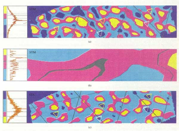
Fig. 5: Color-coded representation of a 7x7 silicon (111) investigation in 1985 (courtesy of IBM research center Zürich, reproduced from Binnig, Rohrer 1986)
In contrast to the gray-scale image in earlier publications on 7 x 7 silicon (111), only four shades of admittedly garish, artificial colors were selected. This type of coding with only a few colors was used several times in scanning tunneling microscopic images in the 1980s, but it did not become standard. The high z-direction resolution obtained with scanning tunneling microscopes could not be adequately represented by a small selection of colors. In these images, the comparison between 'topographic images' and electrical properties stood in the foreground. The earlier suggestion of a 'surface landscape', which conforms to macroscopic visual conventions, was replaced by a design and coloring that create the impression of artificiality.
Click here for larger image.
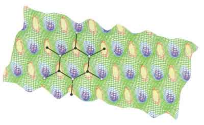
Fig. 6: Representation of a graphite measurement using colors and three-dimensionality (courtesy of IBM research center Zürich, reproduced from Binnig, Rohrer 1986)
In the same article, Binnig and Rohrer describe another study they had made on the surface of graphite (Fig. 6). In this study they used a completely different type of image design. The representation includes both implied three-dimensionality and the use of colors. Here, the individual lines do not point to the scanning of the probe tip. Instead, a mesh forms a surface representing points of equal tunneling current between the tip and the investigated surface. The heights were given a geographical color code consisting of only five colors: The lowest points are dark blue, followed by light blue. Then come green 'mountains' that rise into brown and are finally topped by 'snow-covered' peaks. 6 The detail section floats freely in front of a white background, whereby the external form strengthens the impression of perspective. In addition, geometric figures, black and white circles that are connected to each other by lines, are laid over the mesh. Thus, one can discover several characteristics of the visualization of computer simulations in this image: In simulations, calculations are made for defined points on the grid and the results of the next-closest grid points are graphically connected to each other. For that reason a mesh is used. The free floating in space, the use of garish, unambiguous colors and the application of geometric codification can also be found in visualizations done in the context of simulations ( Warnke 2002 ). The image was designed by Erich Stoll, who had been employed at IBM Rüschlikon since 1970 and who had worked on computer simulations until 1982. Since 1982, he had been responsible for the visualization of STM data. He had acquired his know-how in other research areas and transposed their customary design models onto STM images. Nevertheless, such grid representations did not gain long-term acceptance and were only published a few times. The technical effort and the necessary know-how were probably factors hindering their widespread application, but it is also likely that there was no interest in making measurements done with the scanning tunneling microscope look like simulations.
This investigation of graphite showed that the presence of individual atoms led to a raising or lowering of the tunneling current, according to which electronic states the electrons occupied. That is, the tip is drawn downwards or pushed upwards, in order to keep the tunneling current constant. This interpretation of the image relies on crystallographic knowledge about the atomic lattice of graphite. In contrast to the measurement of 7 x 7 silicon, the atomic structure cannot be derived by counting the maxima. Instead, the familiar atomic lattice is represented by black and white points that correspond to the electrical properties leading to the maximum and minimum in the STM image. According to Binnig and Rohrer's definition, these are topographical images, since the z-position of the tip is given dependent on the ( x , y )-position. However, Binnig and Rohrer put quotations marks around the work "topographical" when they describe this image. They write, "It is in effect a typical spectroscopic image" ( Binnig et.al . 1986 , p. 362). That is, it is an image depicting the electrical properties of the sample. Here, it is shown in the image that the topography of the scanning tunneling microscope cannot be constructed isolated from, but only as a result of measurements of electrical properties.
Although the color selection is reminiscent of a mountain landscape, the grid representation and the circles laid over the image correspondingly show that this is a measurement that is to be interpreted. In the mid-1980s, as the analysis has shown, the creators of the images discussed here chose a form of design that emphasized that the images did not reproduce the surfaces, but, instead, required interpretation.
Apparent reproduction of atoms
As tunneling microscopy became more widespread, further samples were investigated. The physical properties of the samples were not always at the center of attention. In contrast, often well-characterized samples were used as a way to further explore the properties of the tunneling microscope. Randy Feenstra, Joseph Stroscio and their colleagues examined for example GaAs, a III-V semiconductor,at the IBM research laboratory in Yorktown Heights from the mid-1980s. They ascertained that in a scanning tunneling microscopic measurement of a GaAs (110) surface, the gallium atoms could be identified with a maxima and the arsenic atoms with a minima in the STM images. A line representation and a gray-scale representation of the same measurement were published adjacent to each other (Fig. 7). The image was published in 1988 ( Stroscio et.al . 1988 ), as gray-scale images were replacing line images as standard representations. As in the graphite representation from Binnig and Rohrer, in this gray-scale image, the previously known atomic lattice is symbolized by black and white circles for the respective atoms.
Click here for larger image.
Fig. 7: Line representation and gray-scale representation of a GaAs measurement in 1988 (reproduced with permission from Stroscio et al. 1988, © by AVS The Science and Technology Society)
In conformity with theoretical predictions, they were also able to show that when the voltage between tip and surface was reversed, conversely, gallium atoms were associated with minima and arsenic atoms with maxima, when the tip was again guided over the surface under constant current ( Feenstra et.al . 1987 ). Figure 8 shows the results of two measurements with opposite voltage in gray-scale images.
Click here for larger image.
Fig. 8: Representations of two measurements of the same GaAs sample with opposite voltage. (reproduced with permission from Stroscio et al. 1988, © by AVS The Science and Technology Society)
In each image, the square indicates the respective location of the measurement and shows that maxima become minima and vice versa. Feenstra, Stroscio and their colleagues subsequently created a composite image from two measurements with different polarity by using the respective parts that showed the atoms as maxima (Figure 9). They marked the sections of one measurement in red and sections from the measurement with reversed polarity in green. In the publication, they describe the image as follows: "The unoccupied states are colored green, the occupied states are colored red...The calculation shows that the occupied state density is concentrated around the surface As atoms, and the unoccupied density around the Ga atoms" ( Feenstra et.al . 1987 , p. 1193). They thereby show that they have compared the data from their STM measurements with previously existing theory and have interpreted their measurements on this basis. From these considerations they drew the conclusion that the data from their measurements identified the location of individual atoms.
Click here for larger image.
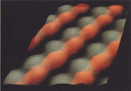
Fig. 9: Combination of two measurements indicated by the use of two colors (courtesy of IBM research center Thomas J. Watson)
A different tenor underlay the description of images from the individual measurements. It states: "Images show either only Ga atoms, or only As atoms." ( Feenstra et.al . 1987 , p. 1193). In this interpretation, only atoms that appear in the image as maxima are visible. Heinrich Rohrer, as well, referred to these measurements in a review article, writing: "As appears in the image of the occupied states, Ga in those of the empty states." (Rohrer 1990, p. 12) Consequently, a minimum, which also arises by keeping the tunneling current between the tip and the individual atom constant, does not show an atom, an atom does not appear . All participants were, of course, theoretically aware that electronic properties determined the trace of the tip and that the minima could be matched to the position of atoms. Nonetheless, even in professional publications they developed a language that deviated from this knowledge and that reserved the visibility of atoms for the appearance of maxima. Here the expectation seems to have prevailed that an atom must appear as an elevation, that is, as a maximum. Seen thus, the composite image is a realization of expectations and thus easy to comprehend. That high aesthetic standards go hand in hand with the fulfillment of this expectation is shown by the color publication in Physical Review Letters , a journal that rarely published color pictures. Compared to the images of earlier STMmeasurements, this image marks a decisive change: No longer is the path of the tip transformed into an image. The individual constituent parts of the measurements have been put together in a manner that suggests an apparent reproduction of the investigated object.
In Feenstra's image individual atoms are visualized according to the expectation that an atom has the shape of a hill or a sphere and not a valley. The image has also been used repeatedly in this sense: Feenstra's IBM colleague, Marc H. Brodsky published the scanning tunneling microscopic composite image, which he had received from Feenstra, in a popular article on GaAs ( Brodsky 1990 ) (Fig. 9). 7
The image's caption reads: "Individual atoms of gallium (green) and arsenic (red) can be recognized in this reproduction done with a scanning tunneling microscope." Although Brodsky was familiar with the history of this image's creation, in the new popular context the composite nature of the image and the visualization of states are no longer mentioned. Instead, this representation of atoms as spheres satisfies the expectations of a broad public and thus does not require explanation. According to the text, this image shows not the results of an examination with the scanning tunneling microscope, but reproductions of atoms themselves. Instead of the original idea of using two colors to distinguish two measurements with two different parameters, in this context the representation implies that different kind of atoms have different colors. This view does not reflect the theoretical knowledge of tunneling microscopists, but this reception was made possible by elaborate image design.
The visualization of an indium phosphide surface designed by Jun Nogami, a post-doctoral researcher in C. F. Quate's work group at Stanford University, had a similar career at the end of the 1980s. In this image (Fig. 10), once again two measurements with opposite polarity between the tip and the surface have been combined into one image in such a way as to allow indium and phosphide atoms to appear as differently colored hills. The measurements and the image design were inspired by one of Feenstra's lectures. Even though there were no plans to publish this image, it belonged to laboratory practice to design and process images in which all atoms took the form of maxima.
Click here for larger image.
Fig. 10: Representation of an indium phosphide investigation; the different colors indicate the use of two different voltages. (reproduced from Forster 1992 with permission from MIT Press)
Although the image was not published in a scientific article at first, because the experimenters felt it was too similar to Feenstra's image, 8 it attracted the attention of John Foster. After receiving his degree from Stanford, Foster had moved to the neighboring IBM laboratory Almaden. In 1989, he lectured at the First Foresight Conference on nanotechnology. In a summary article on scanning tunneling microscopy, which was published in the conference volume ( Crandall & Lewis 1992 ), Foster referred to this image as an example of how different atoms can be distinguished by the scanning tunneling microscope. He mentioned the modification of the applied voltage and the different electrical properties that are measured by the STM ( Forster 1992 , p. 18).
Click here for larger image.
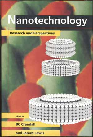
Fig. 11: Cover of the first Foresight-conference volume, combining an STMmeasurement and a computer-generated model. (With permission from MIT Press)
On the cover of the conference volume (Fig. 11), however, a detail section of the image appears in a different context. Here it composes the background to the representation of a computer-generated model of a bearing, which was constructed by the visionaries K. Eric Drexler and Ralph Merkle. Each one of the 2808 atoms in this model is represented by a sphere. The composite image of the two scanning tunneling microscopic indium phosphide measurements and the representation of atoms as hills harmonizes with this utopia. The representation of a nano-scientific examination of the electrical properties of a semi-conductor forms the background of a nanotechnological utopia, which thus seems to enter into the realm of possibility. The combination of both images creates a bridge between utopia and actual science.
Conclusion
For decades, the representation and representability of atoms has undergone constant modification. Discussions between Bohr, Heisenberg, Schrödinger and Born on the representability of quantum mechanics 9 in the 1920s were followed by representations of probability densities, such as those of H. E. White ( White 1931 ). White photographed a rotating needle with extended exposure time and obtained different degrees of brightness, which were supposed to visualize the probability that an electron was located in different orbitals. This tradition was also followed in representations of electron clouds in textbooks from the early 1980s, where they were used to illustrate the inner structure of an atom (Fig. 12).
Click here for larger image.
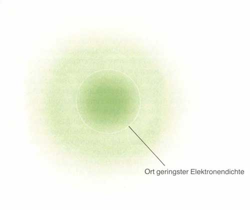
Fig. 12: 'Classical' representation of electron clouds in textbooks in the 1980s. (from: Charles Mortimer: Chemie, 4th ed., Thieme Verlag 1983)
This tradition of representation emphasizes that atoms have no external form, since the locations of the electrons are stated according to probabilities that decrease with increasing distance. The tunneling microscope defines a constant parameter through the tunneling current that guides the tip over the surface at a determined distance. If the image design then no longer suggests that it represents the path of the tip and thus requires interpretation, but instead that the atom itself is being portrayed, the atom can be assigned a form, from which this statement of probability can no longer be derived. In a different pictorial tradition, it goes without saying that atoms are portrayed as spheres, for example in three-dimensional models of crystalline structures (Fig. 13).
Click here for larger image.
Fig. 13: Typical Representation of a Crystal Structure (from: Erwin Riedel: Anorganische Chemie, de Gruyter, 1988)
Interpreted through the theory of signs, these spherical representations are symbols, whose form is determined by convention along. In contrast to this symbolic form of representation, in tunneling microscopic measurements the shape given to the atoms is sanctioned by the instrument. The relationship between representation and object is no longer justified by a convention, but by a measurement. This describes the transition from symbol to icon. This study has aimed to show that this icon is oriented on existing conventions of symbolic representation. In their daily experiments, tunneling microscopists deal with numerous images that have not yet undergone the phases of image design described here, and they must be able to interpret these images. Nonetheless, it is also part of their daily practice to design these images in such a way that they conform to conventional expectations and nanotechnological utopias. Complex image processing and the creation of composite images establish relationships between experimentally sanctioned STM images, for example, and the symbolic representations done by Drexler and Merkle. The status of the tunneling microscope as one of the central instruments in nanotechnology rests on its areas of application and technical possibilities, but also in the power and effect of its images and an image design that emerged out of a dynamic process during the 1980s. 10
References
Baird, D. & Shew, A. "Probing the History of Scanning Tunneling Microscopy." in Baird, D., Schummer, J., & Nordmann, A. (eds.), Discovering the Nanoscale . Amsterdam: IOS Press. 2004, 145-156.
Binnig, G., Rohrer, H., Gerber, Ch., & Weibel, E. "Surface Studies by Scanning Tunneling Microscopy." Physical Review Letters 49 , 1 (1982a): 57-60.
Binnig, G. & Rohrer, H. "Scanning Tunneling Microscopy." Helvetica Physica Acta 55 (1982b): 726-735.
Binnig, G., Rohrer, H., Gerber, Ch., & Weibel, E. "7 x 7 Reconstruction on Si (111) Resolved in Real Space." Physical Review Letters 50 , 2 (1983): 120-123.
Binnig, G. & Rohrer, H. "Scanning tunneling microscopy." IBM Journal of research and Development 30 , 4 (1986): 355-369.
Binnig, G. & Rohrer, H. 1997 "Scanning tunneling microscopy - from birth to adolescence." in: G. Ekspong (ed.), Nobel Lectures, Physics 1981-1990 , World Scientific Publishing Co., Singapore. 1997, 389-409.
Boehm, G. "Die Wiederkehr der Bilder." in Boehm, G. (ed.), Was ist ein Bild ? Fink: München 1995, 11-38
Bredekamp, H. "Drehmomente - Ansprüche und Merkmale des Iconic Turn." in Maar, Ch. & Burda, H. (eds.), Iconic Turn - Die Neue Macht der Bilder . DuMont, Köln, 2004.
Brodsky, M. H. "Progress in Gallium Arsenic Semiconductors." Scientific American 262 , 2 (1990): 68-165.
Crandall, B.C. & Lewis, J. (eds.) Nanotechnology - Research and Perspectives . MIT Press: Cambridge (Mass.), London, 1992.
Feenstra, R.M., Stroscio, J.A., Tersoff, J., Fein, A.P. "Atom-Selective Imaging of the GaAs (110) Surface." Physical Review Letters 58 , 12 (1987): 1192-1195.
Forster, J. "Atomic Imaging and Positioning." in Crandall, B.C. & Lewis, J. (eds.) Nanotechnology - Research and Perspectives . MIT Press: Cambridge (Mass.), London. 1992, 15-36.
Gugerli, D. & Orland, B. (eds.). Ganz normale Bilder , Chronos, Zürich, 2002.
Hansma, Paul K. (ed.). Tunneling Spectroscopy. Capabilities, Applications, and New Techniques. Plenum Press: New York, 1982.
Heintz, B. & Huber, J. (eds.). Mit dem Auge denken , Springer: Wien
Hentschel, K. Mapping the Spectrum . Oxford University Press, 2002.
Hessenbruch, A. "Nanotechnology and the negotiation of novelty." in Baird, D., Schummer, J., & Nordmann, A. (eds.), Discovering the Nanoscale . IOS Press: Amsterdam. 2004, 135-144.
Latour, B. "Der »Pedologen-Faden« von Boa Vista - eine photo-philosophische Montage." in Latour, B (ed.), Der Berliner Schlüssel , Akademie Verlag: Berlin. 1996, 191-248
Latour, B. & Weibel, P. (eds.). Iconoclash. Beyond the Image Wars in Science, Religion, and Art , ZKM and MIT Press, Karlsruhe and Boston, 2002.
Lynch, M. & Woolgar, St. (eds.) Representation in Scientific Practice , MIT Press, Cambridge, Mass., 1990.
Miller, I.A. "Visualization Lost and Regained: The Genesis of Quantum Theory in the Period 1913-27." in Wechsler, J. (ed.). On aesthetics in Science . The MIT Press, Cambridge (Mass.). 1978, 73-104.
Mitchell, W. J. T. "The Pictorial Turn." Artforum , March 1992, 89-94
Pang, A. S.-K. "Visual representation and post—constructivist history of science." Historical Studies in the Physical and Biological Sciences 28 (1997): 139-171.
Rasmussen, N. Picture Control. The Electron Microscope and the Transformation of Biology in America 1940 - 1960 . Stanford University Press: Stanford, 1997.
Stoll, E. "Information- and image-processing of scanning-tunneling-microscope data." SPIE 599 (1985): 442-450
Stroscio, J. A., Feenstra, R.M., Newns, D.M., & Fein, A.P. "Voltage-dependent scanning tunneling microscopy imaging of semiconductor surfaces." Journal of Vacuum Science & Technology A 6, 2 (1988): 499-50gg
Warnke, Ph., Computersimulation und Intervention: Eine Methode der Technikentwicklung als Vermittlungsinstrument soziotechnischer Umordnungen . PhD Thesis, TU Darmstadt, 2002.
White, H.E. "Pictorial representations of the electron cloud for hydrogen-like atoms." The Physical Review 37 , 11 (1931): 1415-27.
Notes
1 For an overview of this topic see the more recent works of Lynch & Woolgar (1988) ; Pang (1997) ; Gugerli & Orland (2002) ; Heintz & Huber (2001) ; Hentschel (2002) ; Rasmussen (1997) ; Latour & Weibel (2002) .
2 The probably most influential contribution on this topic is Latour (1996) , Cf. also various articles in Lynch & Woolgar (1990) .
3 For a review of developments since the declaration of the iconic and pictorial turns see Bredekamp (2004) .
4 Although it is not my intention to perpetuate the tradition of unnamed assistants in this paper, for the sake of readability, I will be naming only the experimentators.
5 Tunneling spectroscopic measurements already existed before the introduction of scanning tunneling microscopes, but they did not have electrode tips like STMs. These tips made a higher local resolution of spectroscopic measurements possible. For an overview of the current state of research on tunneling spectroscopy at the time of the development of the STM, cf. Hansma (1982) .
6 Erich Stoll, who was responsible for the design of this image, mentioned elsewhere ( Stoll 1985 ) that he consciously chose color codes used in cartography.
7 In an email from June 23, 2003, Brodsky told the author that he was familiar with Feenstra's work and that Feenstra had given him this image. It was the first scanning tunneling microscopic image in Scientific American , that was not part of an article directly on scanning tunneling microscopy.
8 In an email from August 21, 2003 to the author, Nogami stated that he had seen the GaAs image at one of Feenstra's lectures and that he had subsequently prepared the indium phosphide measurements without discussing the material with the Feenstra group. That the image was circulated despite its lack of publication is due, in his assessment, to the fact that Quate often passed around the latest images or that his colleague, Park, had used it for advertisement purposes after he founded his SPM firm, Park Instruments .
9 For this discussion cf. Miller (1978) .
10 I thank Elizabeth Neswald for the translation of the text and the anonymus referees for their valuable hints.